The schematic for the DDS signal generator can be found here (click on the image to load the PDF):
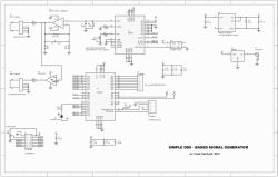
You can see there isn’t a lot on the schematic – it’s pretty simple.
Power
Power comes in through a power jack of your choice, then into a 7805 linear regulator. The +5V is used to power the DDS chip U6, as well as to power the LCD display (in my case it so happened the LCD display I had required 5V). The 5V also powers the sine wave op-amp U5.
5V is also fed to a 3.3V linear regulator U1, and the resultant 3.3V is used to power the Xmega U3 plus the square-wave schmitt trigger U8. Note that the Xmega is not 5V tolerant – it must be powered from 3.3V or less.
Decoupling capacitors are important. The Xmega doesn’t draw a lot of power, but the DDS chip does, as does the sine-wave op-amp. Having plenty of decoupling capacitors up-close to those two chips is important. The schmitt trigger can also draw some current.
DDS Chip & Outputs
The Analog Devices AD9851 is an easy-to-use basic DDS chip. It has some very nice features which really help in this design.
The first is that it contains an internal x6 PLL. So we only need to feed it a slower external clock, 24 MHz in this case, and the DDS will internally multiply that up to 144 MHz for use driving its DAC. This is much easier than trying to feed the part a 144 MHz clock externally.
The chip can be programmed in either a parallel or serial mode. In this design the part is configured for serial mode, which makes for an easy PCB layout as only a few signals need to be run. And we only ever write to the chip – there’s no need to read from it, which means we don’t need to worry about the Xmega being exposed to 5V from the DDS chip.
Finally, the DDS has a current-mode output DAC, where the current is controlled by a resistor on its Rset pin, pin 12. By placing a potentiometer R3 here we can easily change the DDS output level.
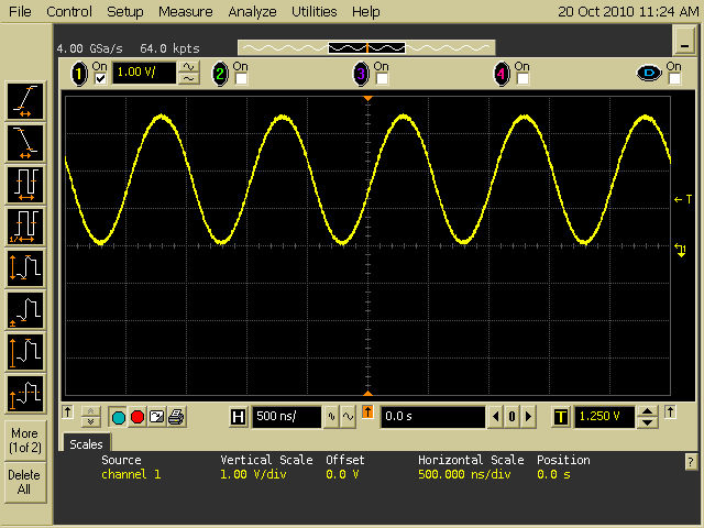
The output from the DDS is fed through a resistor R8 to convert the current to a voltage. C5 provides a small amount of filtering to help the op-amp when the DDS DAC is switching. If you see glitches on the sinewave output you can try increasing C5 a little. From there the voltage on R8 is presented to a non-inverting op-amp U5 with a voltage gain of 1.33 (gain = 1 + R10/R9). This allows us to get close to a 5V p-p output level. C8 is a small capacitor of value 12 – 20 pF or so, to help the op-amp maintain stability. R1 is a resistor to ground to help provide the op-amp with a least a little bit of resistive load. The sine wave is then fed to connector J4. This is an example of what the sine wave looks like at 1 MHz (click on image to make it larger):
The sine wave is also fed to the input of U8, the schmitt trigger. This component is powered from 3.3V but is 5V tolerant, and will output a 3.3V square wave to connector J5. Changing the output level of the sine wave (via R3) will change the duty cycle of the square wave. If the sine wave amplitude is too low, the input threshold voltage of U8 is never reached and there won’t be any square wave output. For higher sine wave amplitudes the sine wave will oscillate above and below U8’s input threshold voltage resulting in a square wave output. In practice I’ve found the duty cycle can be adjusted from around 35% to 70% or thereabouts. This is an example of what the square wave looks like at 1 MHz (click on image to make it larger):
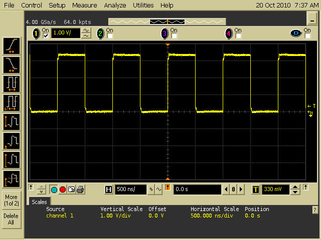
You can see a little dimple at the top of the rising edge and bottom of the falling edge – this is roll-off caused by R12. Reducing R12 reduces this roll-off but too little R12 results in overshoot, which can potentially damage whatever you’re driving. Too much R12 can really start rounding off the square wave. In my opinion the current setting is about optimal, but if you want to fiddle with it, R12 is the part to adjust.
Note that everything in the signal chain is DC coupled – there are no series capacitors. This allows the unit to generate a 1 Hz signal if that’s what you want. On the flip side, there is a DC offset on the sine wave output – it’s not centred around zero because it cannot go negative – this design uses only a +5V positive supply voltage. You can obviously add your own series capacitor on the output if you need the sine wave to be centred around 0V.
Output series resistors R11 and R12 are important for impedance matching to whatever cable is plugged into the unit, as well as for controlling ringing / overshoot on the square wave output.
If you read the AD9851 datasheet, you’ll see some pretty interesting output filtering in some of their examples. Filtering that this design does not have. This filtering is important to achieve optimal SNRs and SFDRs, which I don’t really care about too much for this simple application. The extensive filtering becomes more significant at higher output frequencies. Consider that we’re running the DDS DAC at 144 MHz. For a 10 MHz output signal that’s 14.4 DAC samples per output cycle. At that sampling rate you can start to see the “steps” in the output sinewave waveform, and some fancy filtering can help smooth things out. Such filtering is not trivial to design or implement, which is why it’s not in this design. At lower output frequencies there are so many DAC samples per output cycle it’s simply not a big deal.
Inherent in how it works, a DDS generates not only the specified output frequency, but also spurious output frequencies Fclk, Fclk-Fo, and multiples of these. The photo below is of a spectrum analyzer, with the signal generator outputting a 20 MHz sine wave. (Click on the photo to enlarge it.)
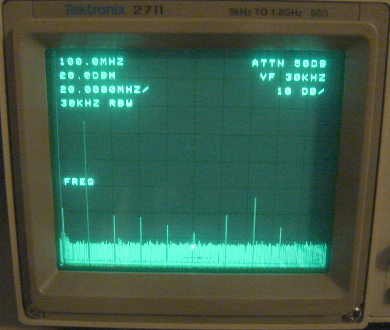
The spectrum analyzer is set to 20 MHz per division, with the far left hand side being 0 Hz. So that spike you can see on the far left, to the left of the word “FREQ” is the DC component. Then the spike on the first division, between the E and Q in “FREQ” is our 20 MHz fundamental. After that you can see the various spurious signals, with a larger one at 144 MHz which is the clock frequency.
In an ideal world we would only see the DC component and the 20 MHz signal; we wouldn’t see the spurs. Low-pass filtering would get rid of these spurs, however some care must be taken. Using a simple low-pass filter it must be designed to permit the highest-possible fundamental frequency to get through. For example 40 MHz. This means that when a lower frequency is generated, for example 1 MHz, its harmonics will be able to pass through the filter (up to 40 MHz in our example). So a simple fixed-frequency low-pass filter is not an optimum solution, but it certainly can help. In this design, the extent of the low-pass filter is limited to C5. (C8 will not have a great effect because it can only reduce the op-amp gain to 1.) Keep things in perspective though. Even that largest spur, at 144 MHz, is almost 30 dB below our 20 MHz fundamental, so for my application as a simple low-cost signal generator it’s not a big deal. Still, depending upon your application, you may wish to consider more output filtering.
LCD
The LCD is a standard HD44780-compatible LCD display. The one I happened to have was a 2×24 character without backlighting, so that’s what I used. Any similar LCD can be used – if you use a smaller display you’ll need to edit the siggen.c software slightly to shorten the strings being written to the screen. My LCD uses a 2×7 header, but some I’ve seen use a straight 1×14 header; your display might be different.
The LCD is configured for 8-bit parallel data, and it’s only written to (the R/W pin, pin 5 in this case) is tied low. In my case the LCD is powered from 5V, so not having to read from it means the Xmega doesn’t have to worry about being exposed to 5V.
Keypad
Keypad is a standard matrix keypad, no diodes or resistors, either 3×4 or 4×4 in size. In my case I used a 3×4. The Xmega contains internal pull-down resistors so we use those to avoid having to put resistors on the board.
Xmega
I used an Atmel Xmega16 because that’s what I had – the code size is small so either a smaller or a larger part would do equally well. The UART TX and RX pins were bought out to test points. The software writes out the UART but that was only for initial debug – once the LCD works it’s easier to just use that. An LED is on the schematic because it’s always fun to have an LED, but it’s not actually used – you don’t need to populate it. J6 the programming header is of course used to program the part.
That’s about it for the hardware. A really basic power supply, an Atmel Xmega driving a DDS chip and an LCD, reading from a matrix keypad. Then the whole thing was put in an off-the-shelf metal box. Easy!
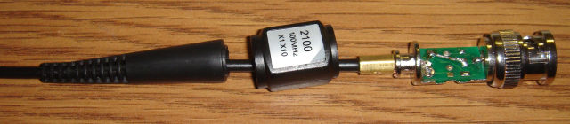
Signal Generator Probe
Sometimes a probe, similar to an oscilloscope probe, can be handy for hooking up the signal generator to a board or chip. A scope probe cannot be used as-is due to the resistors built into the probe. To see how to quickly modify a cheap scope probe, take a look at this blog posting.